What We Offer
End-to-end PCB design services tailored to your needs
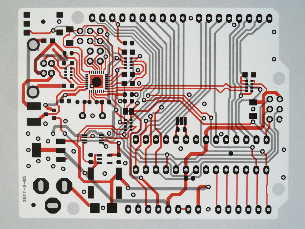
PCB Layout Design
Professional multi-layer PCB layout with optimized component placement, efficient routing, and proper stack-up design. From 2-layer prototypes to 32+ layer high-density boards, we handle projects of any complexity.
- Multi-layer PCB design (up to 32+ layers)
- HDI and microvia technology
- Impedance-controlled routing
- Thermal management solutions
- Design for manufacturability (DFM)
High-Speed Design
Expert signal integrity analysis and high-speed interface design. We ensure your designs meet performance requirements for DDR4/5, PCIe Gen4/5, USB 3.x/4.0, HDMI, and other demanding protocols.
- Signal integrity simulation (SI)
- Power integrity analysis (PI)
- EMC/EMI optimization
- Differential pair routing
- Length matching and timing analysis

Schematic Design
Professional schematic capture with clear hierarchy, proper annotation, and design rule compliance. We create organized, readable schematics that streamline your development process and ensure design accuracy.
- Hierarchical schematic design
- Component selection support
- Design review and optimization
- BOM generation and management
- Complete documentation package

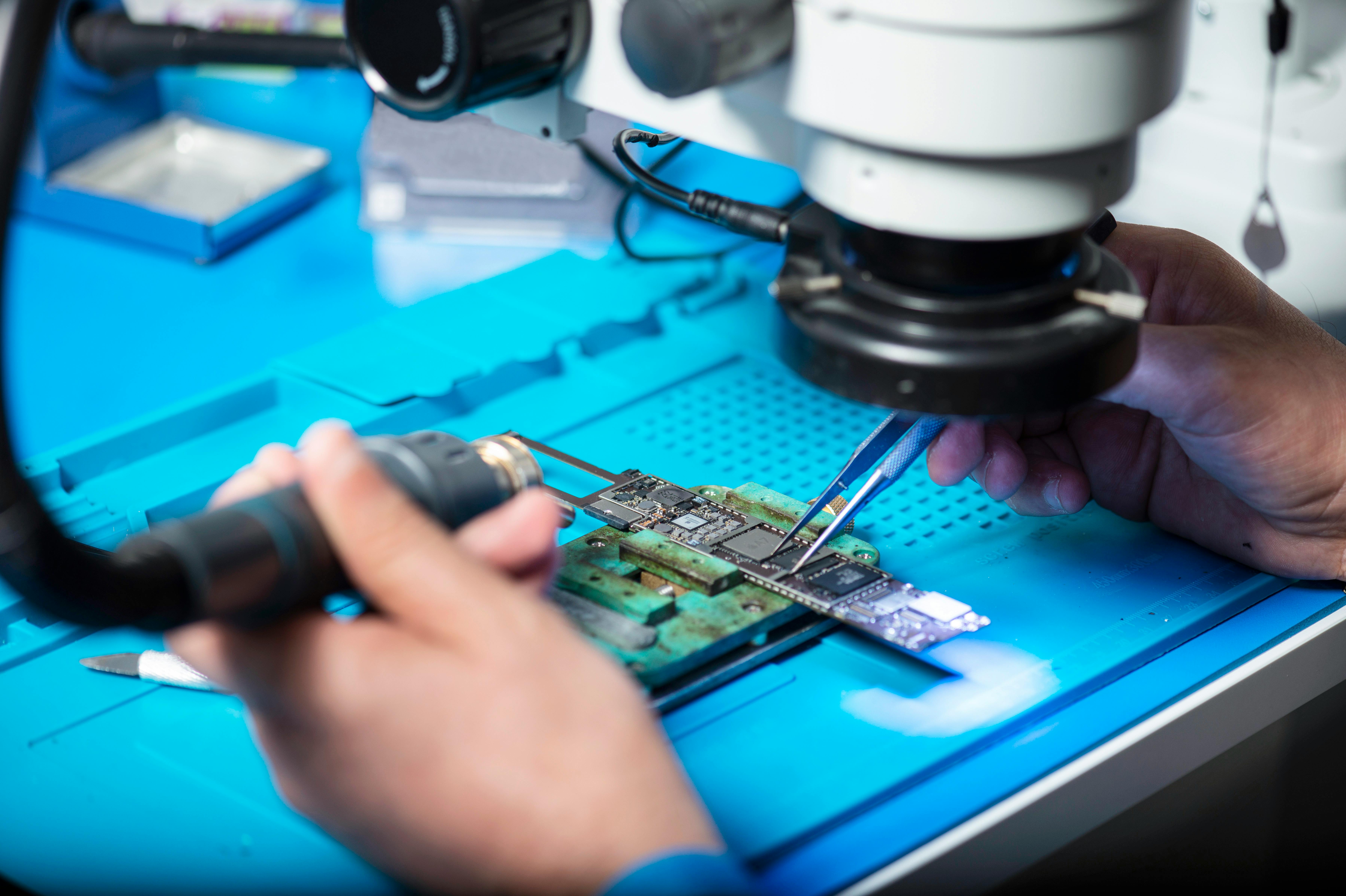
Footprint & Library Services
Custom component footprint creation following IPC standards. We build accurate footprints with 3D models, ensuring perfect fit for your components and smooth manufacturing.
- IPC-compliant footprint design
- 3D model integration
- Library management and organization
- Component verification
- Legacy library migration
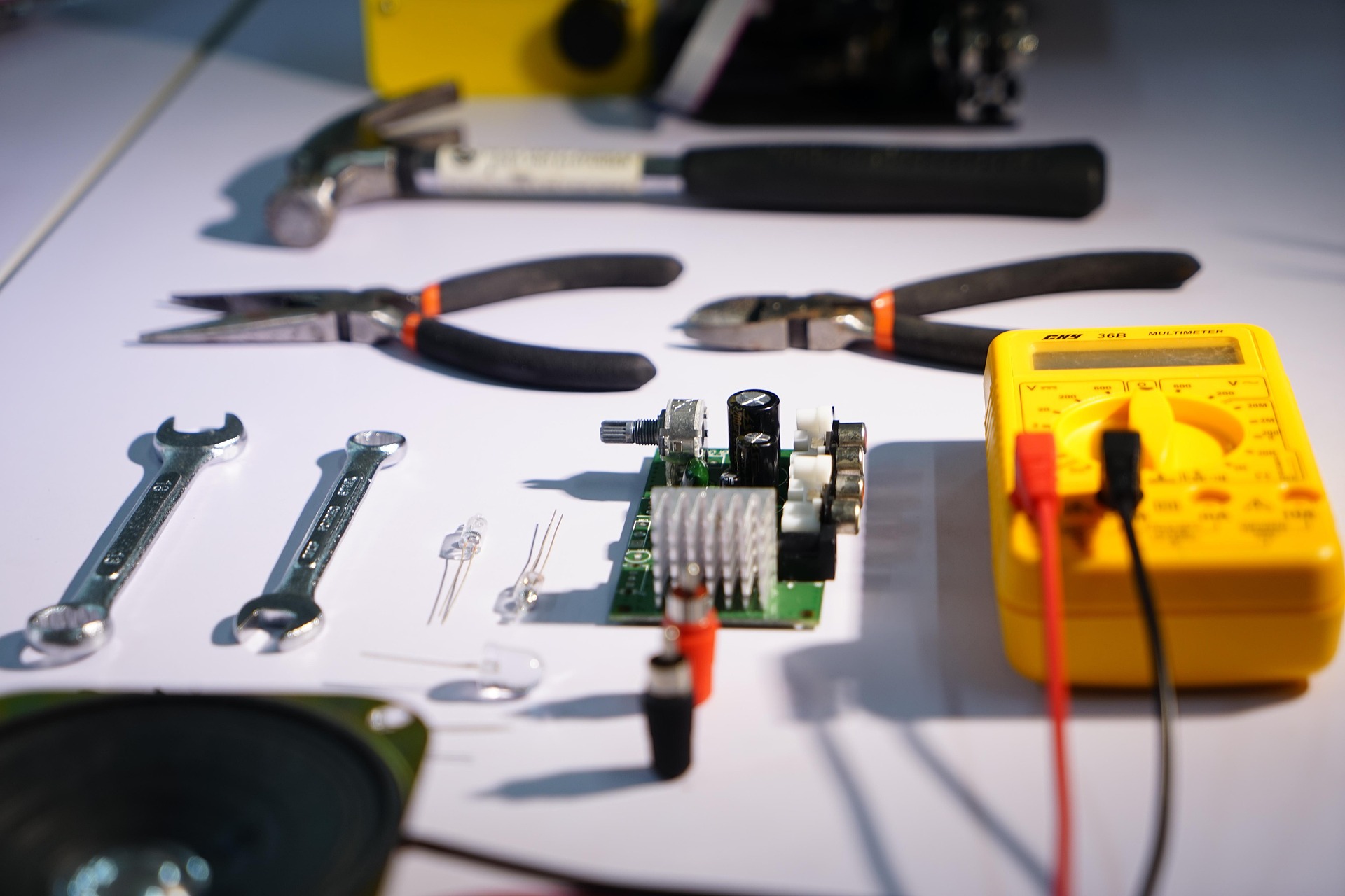
Purchasing & Outsourcing
Streamline your supply chain with our comprehensive purchasing and outsourcing services. We source quality tools, equipment, and electronic components from trusted suppliers worldwide, ensuring competitive pricing and reliable delivery.
- Component sourcing and procurement
- Equipment and tools acquisition
- Vendor management and negotiation
- Quality assurance and verification
- Global supplier network access